Ultra-low Quiescent Current: 0.8μA(VIN=12V)
Shutdown Current: 0.01uA
Input Range: 2.8V-20V
Output Range: 1.8V-5V (0.1V interval)
High Precision: ±2%
Maximum Output Current: 500mA
Enabling Control
Output Discharge
Output Short Circuit Protection
Thermal Shutdown
Low quiescent current: 5μA
Output voltage range: 2.5V~5.6V (step 0.1V), 12V
High accuracy: ±2%
Dropout voltage: 900mV @VOUT=3.3V / IOUT=150mA
Maximum output current: 150mA
Input voltage range: maximum 36V
Output short circuit protection
Thermal shutdown
Overcurrent protection
Input Voltage Range:1.4V-5.5V
Output Voltage Range:0.9V-3.3V,step 0.1V
Output current:500mA
Quiescent current:50μA(Typ)
Shutdown current: < 1μA
Dropout voltage: 120mV@IOUT=300mA,VOUT=3.3V
PSRR: 78db@1kHz,VOUT=1.8V
Low Output Voltage Noise: 29.6uV@VOUT=1.8V
Output voltage accuracy: 1%
Short circuit protection
Ultra-low quiescent current: 2.5μA
High accuracy:±2%
Low dropout voltage:50mV @ IOUT = 100mA @ VOUT =3.3V
Maximum output current:1A
Input Voltage Range:Max 12V
Maximum Output Current:500mA
Low dropout voltage:80mV @ IOUT = 100mA, VOUT =5V
Maximum output current:300mA
Input voltage range:Max 20V
Enabling control
Ultra-low quiescent current: 1.2μA
High accurate:±2%
Low dropout voltage:200mV@IOUT=100mA, VOUT =3.3V
Input Voltage Range:Max 36V
Ultra-low quiescent current:600nA
Standby current:≤10nA
High precision:±2%
Low dropout voltage:60mV @ IOUT = 100mA @ VOUT = 3.3V
Maximum output current:500mA
Input voltage range:Max 6.0V
Enable control
Foldback current limit protection
Low static current: 6μA
Differential pressure:500mV @ IOUT = 100mA @ VOUT =5V
Input voltage range: Max. 35V
Internal Thermal Overload Protection
Internal Short-Circuit Limiting
Recommend Capacitor: 1μF~10μF
CV/CC adjustment error ±%5
No need for optocoupler and 431
Built-in line compensation for more accurate CC adjustment
Built-in Leading Edge Blanking (LEB)
Cycle-by-cycle current limit
Output overcurrent protection
OTP protection
VCC undervoltage and overvoltage protection
Maximum power 12W
Meets Grade 6 energy efficiency standards
Standby power consumption less than 75mW
Wide input AC range: 90Vac~265Vac
Output power: 3~5W
Up to 70KHz operating frequency
Excellent system ESD performance
Adjustable cable compensation(3%~8%)
Adjustable line compensation
High Efficiency Quasi Resonance Mode
Over temperature protection
Output over-voltage protection
CV/CC adjustment error ±5%
Control circuits without optical coupling and all secondary CV/CC component
Quasi resonant working mode
Built-in line compensation for more precise CC regulation
Lead Edge Blanking (LEB)
Periodic Current Limit
VCC undervoltage locking (UVLO) with hysteresis
Built-in short circuit protection and output overvoltage protection
Built-in over-temperature protection
Output power up to 15W
Output power up to 30 W
Output power up to 30W
Built-in 900V power MOSFET
Built-in high-voltage startup circuit
Built-in line voltage compensation and slope compensation
Integrated frequency extension technology
PWM/PFM/PSM hybrid control mode
No-load power consumption<50mW@230VAC
Complete protection functions (OCP, OLP, UVLO, VDD OVP, OTP)
Up to 95% Efficiency
200mV ±3% Feedback Reference Voltage
1MHz Fixed Operation Frequency
Maximum 25V output
Power Save PFM Mode at Light Load
Soft-start Limits Output Overshoot and Inrush Current
3.5A Cycle by Cycle Current Limit Protection
OVP Protection
Highly integrated, simple periphery
Maximum output power: 3W
4-24V Input Voltage Range
Adjustable switching frequency: 200KHz-2MHz, suitable for small transformer size
Adjustable duty cycle: 50% maximum
Over temperature protection and over current protection
In 1 PMU, 2-Bucks, 1-Boost, 1-SuperCap Charger
Fixed output buck converter: 3.3V/500mA
Adjustable output buck converter: 1V-5V
Boost converter: 12V/300mA
Super capacitor charger: 2.5V/60mA
High Efficiency Pulse Skip Mode at Light Load
Power Down Detection and Indication
Auto-alternated Boost Mode and Charger Mode
Hiccup Mode OCP Protections
Low power consumption, quiescent current <1uA
High detection accuracy
Effective power line noise filtering
Integrated rectifier diode
Integrated voltage regulator diode
Few peripheral components
Wide Power Range: 2.7V to 6V
Low MOSFET On Resistance: Rhs=0.3Ω, Rls=0.15Ω
Forward, Reverse, Coast, or Brake Output Modes
Suitable for wide range MCU control logic
Input logic hysteresis
Wide Power Range: 2.5V to 6V
Peak current limiting protection:2.5A
OCP: 2.5A
Wide Power Range: 4.5V to 24V
Low MOSFET On Resistance: Rhs=0.3Ω, Rls=0.3Ω
Wide Power Range: 4V to 24V
Peak current limiting protection:3.5A
Low MOSFET On Resistance: Rhs=0.4Ω, Rls=0.2Ω
Recommended Supply Voltage Range: 3.5 ~40V
Peak current limiting protection:800mA
Ambient Temperature Range: -40 ~+105°C
Compatible with 3~5V MCU
Input Signal Anti-Noise Processing
ecommended Supply Voltage Range: 5 ~ 36V
Up to 450mA current output when adding 1/20 duty cycle input signal.
Operating Temperature Range: -40 ~+105°C
Operating voltage: 6V to 28V
Large signal bandwidth:> 20MHz
3rd harmonic suppression:40dBc @ 10M / 10Vpp / 50Ωload,50dBc @ 5M / 10Vpp / 50Ωload,60dBc @ 2M / 10Vpp / 50Ωload,76dBc @ 500K / 10Vpp / 50Ωload
2nd harmonic suppression:55dBc @ 10M / 10Vpp / 50Ωload,60dBc @ 5M / 10Vpp / 50Ωload,70dBc @ 2M / 10Vpp / 50Ωload,80dBc @ 500K / 10 Vpp /50Ωload
Operating current externally set, digitally controllable
Slew rate:500 V/μs
Maximum differential output:2x operating voltage -6V@50Ωload
TTL / CMOS compatible
Temperature range -40°C to +85°C
Operating voltage:6V to 28V
Large signal bandwidth:>20MHz
3rd harmonic suppression:> 40dBc @ 10M / 10Vpp / 50Ωload,> 50dBc @ 5M / 10Vpp / 50Ωload,> 60dBc @ 2M / 10Vpp / 50Ωload,> 76dBc @ 500K / 10Vpp / 50Ωload
2nd harmonic suppression:> 55dBc @ 10M / 10Vpp / 50Ωload,> 60dBc @ 5M / 10Vpp / 50Ωload,> 70dBc @ 2M / 10Vpp / 50Ωload,> 80dBc @ 500K / 10 Vpp /50Ωload
Fixed 1/4 duty mode, 1/3bias voltages supporting a maximum of 160 segments
Low power consumption design, 6uA current at typical condition
Incorporates an internal OSC Circuit
Internal LCD Contrast control Circuit
Integrated Power-on Reset Circuit
No external component required
Includes an I2C interface
Compatible with TTL/CMOS
High EMC immunity
Fixed 1/4 Bias, 1/8 Duty.
35*8 = 280 bits, with built-in buffer amplifier.
Low power consumption design, 5uA current at typical condition.
Interface: 2 wire serial interfaces
Integrated reset and oscillator circuits.
Fixed 1/4 duty mode, Up to 192 dots
Built-in OSC Circuit
Fixed 1/4 duty mode, Up to 384 dots
CPU maximum frequency can reach 200MHz
Frequency dynamic switching, effectively reducing power consumption
Built-in encryption and decryption engine
Support JATG online debugging
Support global maskable interrupts
Built-in 1.5M SRAM
Support SPI, support CPU BOOT from SPI port
Support UART and debugging functions
Support general GPIO function
Support 32-bit counter (timer) function
Ethernet chip PHY, equipped with MDIO and RMII ports
Support DMA function
Equipped with hardware watchdog
One-time write eFuse function
State Grid dual-mode (wired-wireless) communication protocol
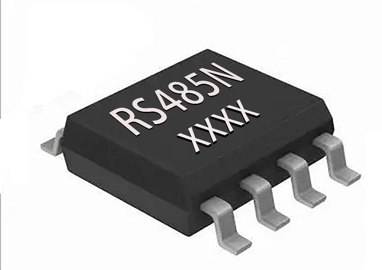
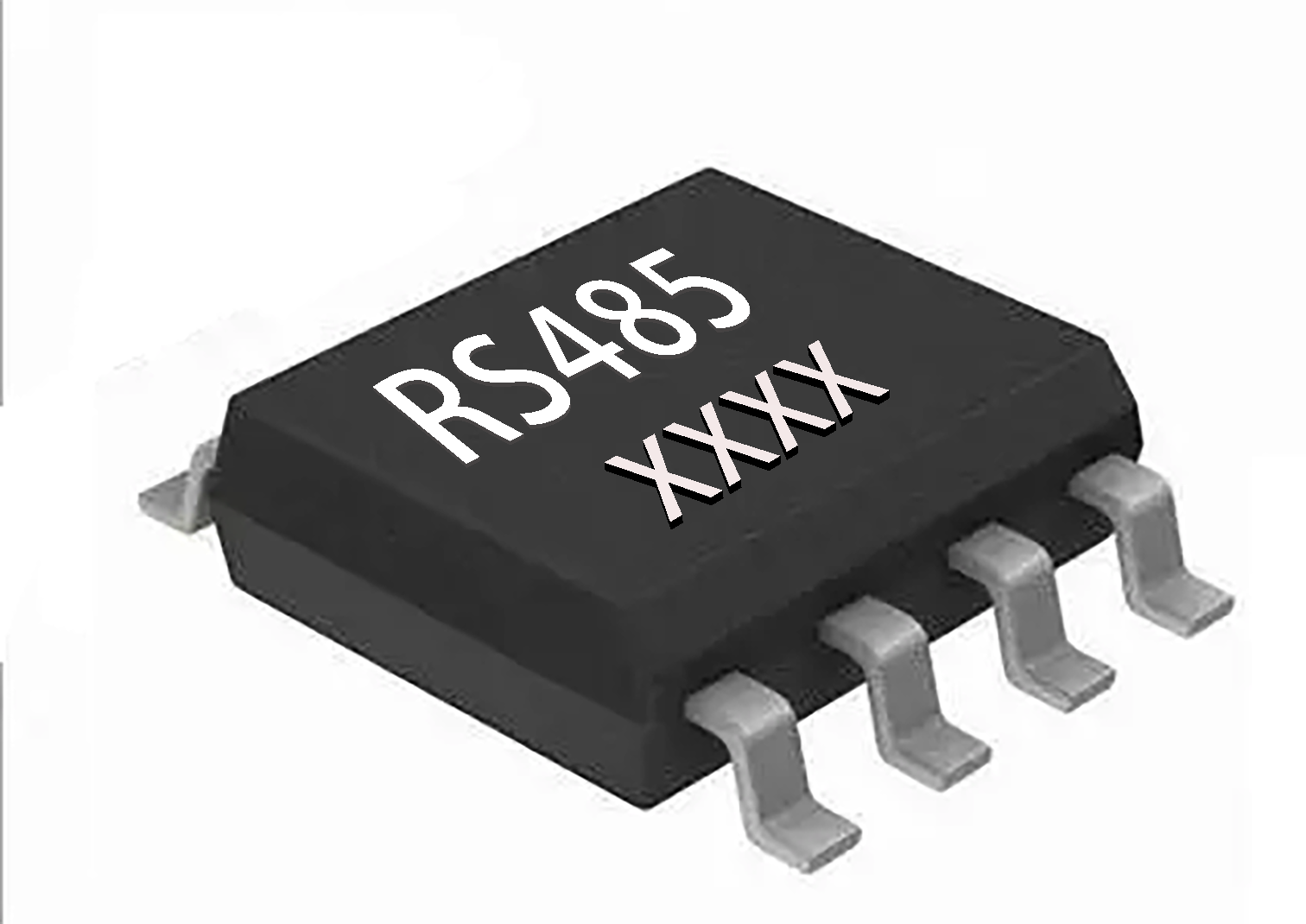
The RS485 is a +5V, half-duplex, ±15KV ESD protected RS485/RS422 transceiver circuit. The circuit contains single channel driver and single channel receiver internally.
The RS485 is a half-duplex type with drive enable (DE) and receive enable (RE) pins. When in the off state, the drive and receive outputs are high resistance.
The RS485 has a fail-safe circuit to ensure correct receiver output when the receiver input is open or shorted.
The RS485 receiver input impedance is 1/8 unit load, allowing up to 256 transceivers to be hooked up to the bus.
3.3V/5V supply voltage
enhanced slew rate limiting helps reduce output EMIand reflections caused by mismatched terminal connections, achieving 500kbps error-free data transmission
Communication ports provide ±15kVHuman Body ModelESDprotection
Roman">Fail-safefunction
With1/8unit load, up to256transceivers can be connected on the same bus
Using Roman">8pinSOpackage
Chip Features
Typical Applications
Ordering Information
025-58270802
021-61090382


 Typical ApplicationsOrdering Information


 Current Location:
 Sample Request
 Product Data Sheet Preview